Delhi’s draft chip policy targets design, R&D and advanced packaging
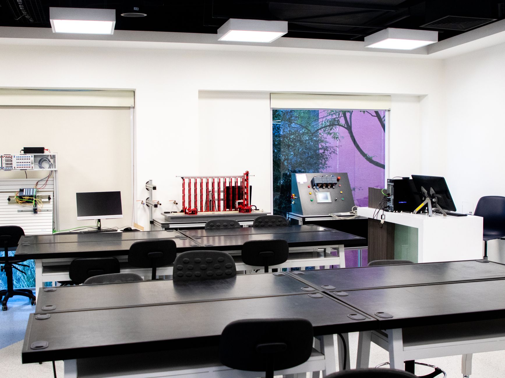
Delhi’s proposed 2026–31 semiconductor policy would prioritise design, testing, research and advanced packaging over large chip-fabrication plants.
Delhi’s draft 2026–31 chip policy proposes ₹63–79 crore for design, packaging, testing, startups and skills.
Delhi’s proposed semiconductor policy would focus on chip design, research and advanced packaging rather than the large wafer-fabrication plants that need substantial land and water.
The 2026–31 draft sets out an indicative budget of ₹63–79 crore, with ₹1 crore proposed as seed funding in 2026–27. It aims to attract investment in fabless chip design, research and development, and assembly, testing, marking and packaging (ATMP) and outsourced semiconductor assembly and test (OSAT) facilities.
For eligible ATMP/OSAT and compound-semiconductor projects, the proposal includes an additional capital subsidy worth 50% of central assistance, capped at ₹50 crore per project. Other proposed support includes five years of lease-rental subsidy, exemptions on stamp duty and electricity duty, and a ₹2-per-unit power-tariff subsidy.
Chip-design startups and MSMEs could receive reimbursement of 20% of eligible design expenditure, capped at ₹15 crore per unit. The policy targets at least two commercialised indigenous chip designs from Delhi-based startups each year, while encouraging talent from IIT Delhi, IIIT Delhi, Delhi Technological University and Netaji Subhas University of Technology to work in the city.
IT minister Pankaj Singh said the government plans to place the policy in the public domain by the end of September after Cabinet approval.
Latest stories
- GMDA hires consultant to link recycled-water pipelines in Gurugram
- Railway Board sanctions trains for Bengaluru Pink Line’s elevated section
- Khalin Joshi takes six-shot lead at Bengaluru Open halfway stage
- MCG gives 24 hours to clear debris from Gurugram public spaces
- Mumbai: S. J. Poddar Academy Grade 6 students curate Zoographia
- Marsh crocodile rescued from 8-foot electricity duct at Aarey Metro complex
- Western Railway says Mumbai division collected 5.2 tonnes in cleanliness drive
- Over 1,000 students exhibit work at Bengaluru children’s biennale
- Delhi to set up 110 collection centres for old and damaged idols
- Mumbai: Nani says The Paradise makers expected an A certificate
- Niranjan Hiranandani shows six-storey Malabar Hill home Kanta
- Mumbai chocolatier makes 75kg chocolate Ganesha idol for Pune
- Heavy vehicles barred on Varthur-Gunjur SH-35 during peak hours
- CSMT inspection: PAC seeks wider north-side entry for evening rush
- Bengaluru Airport T2 hosts ten-day Odia food festival
- Delhi sets up 78 artificial ponds for Ganpati visarjan
- Mahapanchayat backs Gurgaon road-collision accused; biker calls it an attempt to shift the narrative
- Bengaluru Cantonment station redevelopment expected by December 2026
- Railways approves ₹497 crore to double Chouk–Karjat line
- Delhi Metro logs record 82.45 lakh boardings during DTC strike
Cities
- Delhi news
- Gurgaon news
- Noida news
- Greater Noida news
- Ghaziabad news
- Faridabad news
- Delhi NCR news
- Bengaluru news
- Mumbai news
- Navi Mumbai news
- Thane news
Sections
- Top Stories
- Latest
- Politics
- Governance
- Civic Issues
- Transport and Traffic
- Metro
- Roads and Infrastructure
- Weather and Air Quality
- Business and Startups
- Real Estate
- Education
- Health
- Environment
- Courts and Policy
- Safety
- Arts and Culture
- Events
- Things To Do
- Food and Drink
- New Openings
- Shopping
- Nightlife
- Neighbourhoods
- People
- Technology
- Sports
GTK covers the news, people, culture, neighbourhoods, civic life and food shaping India’s cities. Better Starts With Us.